From Moore's Law to the Tau Law: When Chips Chase Time
From Moore's law to the Tau law: chips are no longer chasing density, they are chasing time. This new metric measures how efficiently circuits communicate, and it rewrites what progress means in the AI era.
The Tau Law focuses on the time constant τ (tau), the delay a signal experiences as it moves through a circuit. Instead of compressing more transistors into a smaller area, designers optimise the path signals take, reducing parasitic resistance and capacitance. The practical expression of this idea is an architecture called LogicFolding, which reorganises circuits by folding them into more efficient layouts. According to sources, Huawei targets equivalent densities of 1.4 nm by 2031 and plans to deploy Tau-based designs on Kirin chips as early as 2026.
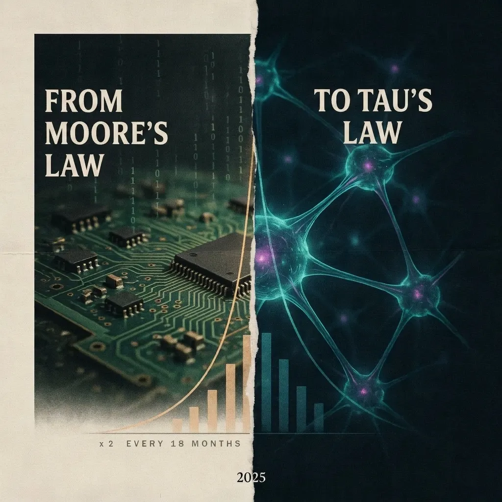
From Moore's Law to Latency: A Change in How We Measure Progress
For nearly sixty years, Moore’s Law taught us to think in terms of geometric scaling: every two years, double the number of transistors per area and halve the cost. That lens made engineers obsessed with shrinking. Tau replaces that lens with one that values latency, energy per operation and systemic efficiency. It does not deny the importance of smaller nodes, but it treats them as one variable among many. The real gain, proponents argue, comes from reorganising how circuits communicate with themselves.
This perspective resonates well beyond semiconductor physics. If progress is measured by the quality of connections rather than the quantity of components, then many fields , from education to artificial intelligence , can learn from the same principle. Accumulating processing power without reducing internal friction is merely brute force. Tau suggests that intelligent architecture often matters more than raw density.
How LogicFolding Reinvents the Chip
LogicFolding works by taking a conventional flat circuit layout and folding parts of it onto themselves, much like pleating a sheet of paper. The goal is to shorten critical signal paths and reduce parasitic effects that slow down communication. This organisation allows the chip to operate at higher frequencies or lower power for the same performance. The technique does not require the most advanced extreme ultraviolet (EUV) lithography tools, which have become a bottleneck for companies like Huawei due to export restrictions.
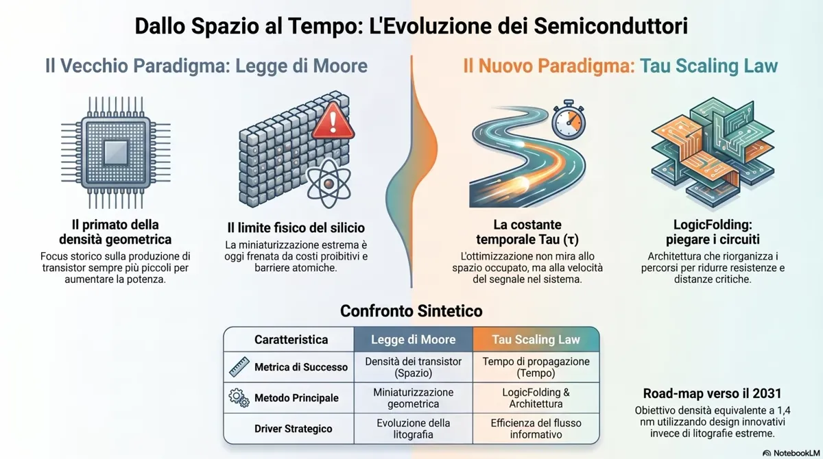
Instead, LogicFolding achieves gains through design innovation rather than process shrinks. It exploits the third dimension of the chip , stacking and folding , to bring logically related components physically closer. This is reminiscent of early 3D integration but applied at the level of standard cells and interconnects. The result is a chip that can deliver the performance of a smaller node while using a more accessible manufacturing process.
“The real innovation is not in silicon alone, but in the mental architecture that guides silicon design.”
A short animated explainer by Centre for Technomoral Futures illustrates how Tau connects component design with ecosystem thinking, showing that what matters is the time a bit takes to become an action.
Tau Law and Geopolitics: Strategic Necessity in the Chip Race
The Tau Scaling Law is not a purely technical invention; it is a direct response to geopolitical constraints. Huawei and other Chinese firms have faced increasingly strict restrictions on accessing the most advanced lithography machines, such as those produced by ASML. Without the ability to shrink transistors below 3 nm using traditional methods, companies must find alternative routes to performance gains. Tau offers a path that is partly independent of lithography limits, reducing dependence on a single supply chain.
This does not mean that Tau will replace traditional scaling entirely. It is plausible that the approach works best in specific domains , such as AI accelerators and mobile processors , where latency and energy efficiency are paramount. General-purpose CPUs may still benefit from continued density scaling where possible. The history of technology warns against absolute formulas. Yet even as a partial solution, Tau changes the conversation: progress is no longer synonymous with shrinking.
A Digital Humanist Interpretation
From a digital humanist perspective, the Tau Law offers a powerful metaphor. For decades, we believed that progress meant compression, speed and centralisation. Today, we see that sustainable advancement often depends on the quality of relations among parts, the elegance of organisation and the reduction of friction in the flow of value. This applies to school systems, information networks and artificial intelligence. Accumulating power is not enough; we must build architectures that allow intelligence to circulate with the least possible resistance.
Conclusion: The Courage to Change Direction
Tau scaling may become a robust new paradigm, or it may remain a brilliant optimisation tool for certain contexts. What is certain is that the metric of advancement is being rewritten. Moore’s Law taught us to ask “how small?”. Tau invites us to ask “how efficiently connected?”. The future, it seems, does not always emerge from running faster in the same direction. Sometimes it requires the courage to change direction completely.
For context: the physics of chips is the quiet engine behind the stories I told in data centers spinning out of control and in AI price disruption: when chips chase time, both cost and energy change.
Frequently Asked Questions
What is the Tau law in chip design?
The Tau law, associated with LogicFolding and similar approaches, measures progress in chip design by communication efficiency and latency rather than transistor density. It treats smaller nodes as one variable among many, not the only goal.
How does the Tau law differ from Moore's law?
Moore's law predicted that the number of transistors on a chip would double roughly every two years, equating progress with shrinking. The Tau law shifts the metric from density to time: how efficiently circuits communicate and how quickly value flows through the architecture.
Why does chip latency matter for AI infrastructure?
AI workloads depend on moving enormous amounts of data quickly between compute, memory, and networks. When communication efficiency becomes the bottleneck, reducing latency and energy per operation matters more than adding raw transistor count, which is why the Tau law is increasingly relevant for AI accelerators.